How to select a suitable wafer inspection lamp.
Author: SUNLONGE Admin
How to select a suitable wafer inspection lamp.
For decades, Halogen lamps are the key player in the wafer surface inspection service. While Halogen lamp is still in use, more and more customers complained about it, eg high body temperature, frequent bulb replacement. Now LED light sources are a new preferred solution for the wafer surface inspection, offering advantage such good efficiency, lower power consumption, less heat and much longer lifespan. Still there are several technical parameters need to be considered when selecting a suitable wafer inspection lamp.
1. High illuminance.
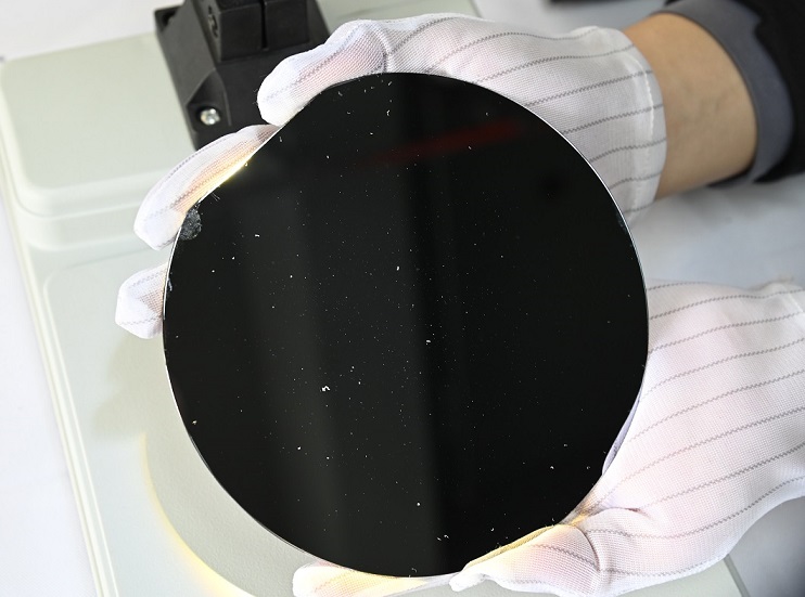
Illuminance is the key factor to consider for the wafer surface inspection. The higher illuminance the lamp is, the better performance will it be. We suggest that the illuminance need to be 200 000 lux at 30cm distance, which should be equivalent with the 200W mercury bulb. Then a lamp can detect the minimal surface defect on the wafer surface.
2. Long lifespan
The mainly complaint about Halogen lamp is the frequent bulb replacement. Usually, you need to replace a new bulb in one month, even hundred hours, which is costly and inefficiency. Meanwhile, LED can be more stable and need less maintains during the lifespan. More important the lifespan is up to 30 000H. Longer lifespan can help the wafer inspection work become easy and secured. It will also help largely cut the related cost in the industry.
3. More secured
Secure is an important factor before your selection. As we know, mercury lamp is with 100-1200C body temperature during the operation. And LED can keep 500C around during the inspection. It makes the LED a much safer and more environment friendly. And illuminance stability of LED can be up to 90%. That is why more and more wafer customers are now turning to the LED during the surface inspection job.
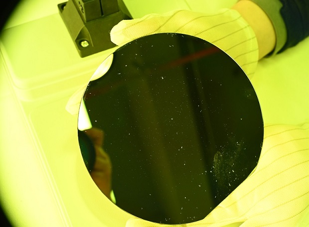
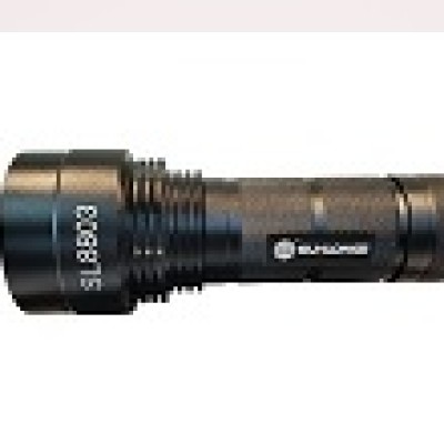
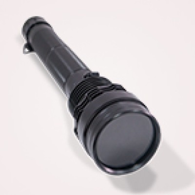
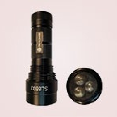
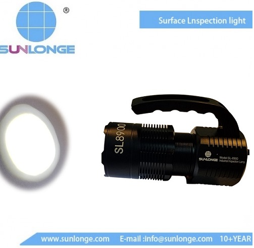
Considering all these issues, Sunlonge SL8900 is suitable and powerful wafer inspection lamp in the current market. SL8900, 30W LED light source with customized optical lens, illuminance up to 400 000 lux at 30CM distance. According to our study, it can detect the defect at minimal 1um size on the wafer surface. As we can see, SL8900 will be the priority for the wafer inspector in the near future.
 CN
CN

